Arizona State University (ASU) and Deca Technologies (Deca), a supplier of superior wafer- and panel-level packaging expertise, introduced a groundbreaking collaboration to create North America’s first fan-out wafer-level packaging (FOWLP) analysis and improvement middle.

Photograph courtesy of Arizona State College.
The brand new Heart for Superior Wafer-Stage Packaging Functions and Improvement is ready to catalyze innovation in the USA, increasing home semiconductor manufacturing capabilities and driving developments in cutting-edge fields equivalent to AI, machine studying, automotive electronics, and high-performance computing.
The middle will mix state-of-the-art advanced-packaging expertise, tools, processes, supplies, experience, and coaching, fostering the event of recent capabilities from proof of idea to pilot scale. ASU is the primary college implementation of Deca’s M-Collection fan-out, and Adaptive Patterning applied sciences beneath the Microelectronics Commons, a community of regional expertise hubs coordinated to ship on initiatives requested by the Division of Protection as a part of the CHIPS and Science Act, the federal laws which goals to develop America’s international management in microelectronics.
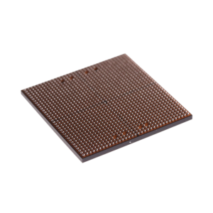
Deca Applied sciences Inc.
The brand new middle will embrace integration with the college’s MacroTechnology Works middle at ASU Analysis Park in Tempe and can present an enhanced functionality that may advance initiatives inside the ASU-led Southwest Superior Prototyping (SWAP) Hub, a part of the Microelectronics Commons.
“That is on the coronary heart of the subsequent era of innovation in microelectronics and the whole lot it allows,” stated Zak Holman, vice dean for analysis and innovation for ASU’s Ira A. Fulton Faculties of Engineering. “Deca has developed a novel expertise, and ASU brings extraordinary capability that may present the assets to leverage Deca’s expertise in ways in which might be a differentiator for the work we’re doing collectively by way of the SWAP Hub.”
The initiative additionally provides a workforce-development alternative with ASU college and college students participating within the work being finished, offering coaching for the rising variety of technicians who’re wanted domestically, together with in metro Phoenix, which is dwelling to Intel, TSMC, Amkor, and different firms.
In collaboration with Deca, ASU is dedicated to establishing onshore entry to those superior packaging capabilities. This entails buying, putting in, and implementing a complete set of course of and metrology tools on the facility, able to accommodating each 200 mm and 300 mm system wafer codecs, in addition to 300 mm M-Collection molded fan-out wafers, offering unparalleled flexibility for a various vary of consumers and functions.
“With the business’s main fan-out expertise as a basis, we’re excited concerning the prospects this new middle brings to Arizona in addition to the broader U.S. semiconductor business,” stated Tim Olson, Deca’s founder and CEO. “By way of ASU and Deca’s collaboration, unprecedented entry for business, academia, authorities, and others opens the door to speed up innovation and bolster U.S. expertise management.”
Deca’s first-generation M-Collection FOWLP is broadly adopted in main smartphones across the globe. The Gen 2 M-Collection together with Adaptive Patterning expertise brings unprecedented scaling to greater densities for heterogeneous integration and chiplet functions.
Photograph courtesy of Arizona State College.
The brand new Heart for Superior Wafer-Stage Packaging Functions and Improvement is ready to catalyze innovation in the USA, increasing home semiconductor manufacturing capabilities and driving developments in cutting-edge fields equivalent to AI, machine studying, automotive electronics, and high-performance computing.
The middle will mix state-of-the-art advanced-packaging expertise, tools, processes, supplies, experience, and coaching, fostering the event of recent capabilities from proof of idea to pilot scale. ASU is the primary college implementation of Deca’s M-Collection fan-out, and Adaptive Patterning applied sciences beneath the Microelectronics Commons, a community of regional expertise hubs coordinated to ship on initiatives requested by the Division of Protection as a part of the CHIPS and Science Act, the federal laws which goals to develop America’s international management in microelectronics.
Deca Applied sciences Inc.
The brand new middle will embrace integration with the college’s MacroTechnology Works middle at ASU Analysis Park in Tempe and can present an enhanced functionality that may advance initiatives inside the ASU-led Southwest Superior Prototyping (SWAP) Hub, a part of the Microelectronics Commons.
“That is on the coronary heart of the subsequent era of innovation in microelectronics and the whole lot it allows,” stated Zak Holman, vice dean for analysis and innovation for ASU’s Ira A. Fulton Faculties of Engineering. “Deca has developed a novel expertise, and ASU brings extraordinary capability that may present the assets to leverage Deca’s expertise in ways in which might be a differentiator for the work we’re doing collectively by way of the SWAP Hub.”
The initiative additionally provides a workforce-development alternative with ASU college and college students participating within the work being finished, offering coaching for the rising variety of technicians who’re wanted domestically, together with in metro Phoenix, which is dwelling to Intel, TSMC, Amkor, and different firms.
In collaboration with Deca, ASU is dedicated to establishing onshore entry to those superior packaging capabilities. This entails buying, putting in, and implementing a complete set of course of and metrology tools on the facility, able to accommodating each 200 mm and 300 mm system wafer codecs, in addition to 300 mm M-Collection molded fan-out wafers, offering unparalleled flexibility for a various vary of consumers and functions.
“With the business’s main fan-out expertise as a basis, we’re excited concerning the prospects this new middle brings to Arizona in addition to the broader U.S. semiconductor business,” stated Tim Olson, Deca’s founder and CEO. “By way of ASU and Deca’s collaboration, unprecedented entry for business, academia, authorities, and others opens the door to speed up innovation and bolster U.S. expertise management.”
Deca’s first-generation M-Collection FOWLP is broadly adopted in main smartphones across the globe. The Gen 2 M-Collection together with Adaptive Patterning expertise brings unprecedented scaling to greater densities for heterogeneous integration and chiplet functions.